Today, let's talk about the LM741 chip, mainly from the following aspects:
1. What chip is LM741?
2. Working principle of LM741
3. LM741 Internal Circuit Explanation
4. LM741 Features and Specifications
5. LM741 chip application field
1、 What chip is LM741?
LM741 operational amplifier is a DC coupled high gain electronic voltage amplifier, which is one of the most commonly used operational amplifier integrated circuits and can perform both digital operations and amplification functions.
The main function of LM741 operational amplifier is to perform mathematical operations in various circuits. Operational amplifiers have significant gain and are typically used as voltage amplifiers. LM741 can operate under single or dual power supply voltages.
The LM741 circuit adopts internal compensation, which is relatively simple and not easily self-excited. Its operation is stable and simple, and it is designed with a complete protection circuit that is not easily damaged.
Due to its high quality and reliable performance, the operational amplifier LM741 is very suitable for comparators, multivibrator, DC amplifiers, summation amplifiers, integrators or Differentiator and active filters.
2、 LM741 Internal Circuit Explanation
The standard operational amplifier IC 741 consists of a circuit consisting of 20 transistors and 11 resistors. All these transistors and resistors are integrated into a single chip.
Here, the inverted and non inverted terminals are connected to transistors Q1 and Q2, respectively. Transistors Q1 and Q2 are both used as NPN emitters. The outputs of transistors Q1 and Q2 are connected to a pair of Q3 and Q4 transistors. This type of configuration isolates the two inputs of transistors Q3 and Q4 and prevents possible feedback.
The voltage fluctuation at the input end of the operational amplifier can affect the current flow in the internal circuit and also affect the effective functional range of the transistors in the circuit. To prevent this from happening, two current mirrors were used. The transistor pairs (Q8, Q9) and (Q12, Q13) are connected in some way to form two mirror circuits.
Transistors Q8 and Q12 are used as adjustment transistors to set the voltage level of the emitter base (EB) junction for the corresponding transistor pair. This voltage level can be accurately adjusted to a few millivolts to allow the required amount of current.
The first mirror circuit developed by Q8 and Q9 is coupled to the input circuit, while the second mirror circuit developed by Q12 and Q13 is coupled to the output circuit. In addition, the third mirror circuit developed by Q10 and Q11 serves as a high impedance connection between the input and negative power supply. The reference voltage it provides has no load impact on the input circuit.
3、 Working principle
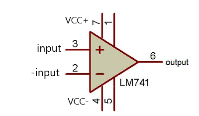
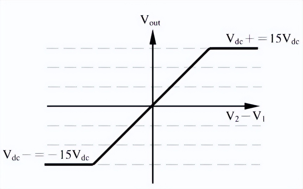
When using LM741, it is necessary to provide a pair of equally sized positive and negative power supply voltages+Vdc and - Vdc on pins 7 and 4. Once there is a voltage difference between pins 2 and 3, that is, between the two input terminals, the voltage difference will be amplified at the output terminal.
The operational amplifier has the characteristic that the output voltage value will never be greater than the positive supply voltage+Vdc or less than the negative supply voltage - Vdc. If the input voltage difference is greater than the range of external power supply voltage+Vdc to - Vdc, its value will be equal to+Vdc or - Vdc.
The basic operation of LM741 is shown in the following figure. If a voltage is input at the same phase input terminal, an amplified output of the same polarity will be obtained at the output terminal; If the same voltage signal is input at the inverted input end, a signal output with the same amplification factor but opposite polarity will be obtained at the output end.
When inputting voltage to both input terminals of the amplifier at the same time, subtracting the voltage value (V2) of the opposite input terminal from the voltage value (V1) of the same phase input terminal can obtain the ratio of output multiplied by output terminal (V1-V2).
Transistor Q16, together with resistors 4.5K Ω and 7.5K Ω, forms a voltage level converter circuit, which reduces the voltage level of the input amplifier circuit by Vin and then transfers it to the next circuit. This is done to prevent signal distortion in the output amplifier section.
Transistors Q15, Q19, and Q22 are designed as Class A amplifiers, while transistors Q14, Q17, and Q20 form the output stage of operational amplifier IC 741.
In order to balance any irregularity in the input phase of the differential circuit, transistors Q5, Q6, and Q7 will form a configuration with Offset null+ve and - ve, and balance the inverted and non inverted inputs accordingly.
4、 LM741 parameters
The input impedance is greater than 100K Ω.
The output impedance is less than 100 Ω.
The frequency range is between 0HZ and 1MZ.
Low offset voltage and current.
The voltage gain is approximately 2,00000.
Power supply: In order to function properly, it requires a power supply of at least 5V and can handle voltages up to 18V.
Input impedance: approximately 2 M Ω.
Output impedance: approximately 75 Ω.
Voltage gain: The minimum frequency range is 2,00000.
Conversion rate (operational amplifier can detect the rate of voltage change): 0.5V/µ s.
Input offset: within the range of 2mV-6mV.
Output load: It is recommended to exceed 2K Ω.
Maximum output current: 20 mA.
Note: In order to use the operational amplifier as a voltage amplifier, it is recommended to use high input impedance and low output impedance values. This impedance makes the operational amplifier IC 741 an almost ideal voltage amplifier. The above specifications are universal and may vary depending on the manufacturer.
5、 Application field:
Advertising conversion on our mobile phones, in audio amplifiers, programmable logic controllers, video signal conditioning units, processors, sensor data control, digital to analog converters in phones, temperature sensors and controllers, error amplifiers, communication circuits, mobile phone chargers, receivers, modulato.
![]() Contact-us
Contact-us