Today, the TOPCHIP Electronics small classroom was launched, discussing the working principles of MOS transistors.
1、 What is a MOS transistor?
MOSFET is a type of FET with insulating gates, where the voltage determines the conductivity of the device. The invention of MOS transistor is to overcome the shortcomings of FET, such as high drain resistance, medium input impedance, and slow operation. So mos transistors can be referred to as advanced forms of FETs.
MOSFETs are often used for switching or amplifying signals. The ability to change conductivity with the applied voltage can be used to amplify or switch electronic signals.
MOSFETs are by far the most common transistors in digital circuits, as memory chips or microprocessors may contain hundreds or millions of transistors. Since they can be made of p-type or n-type semiconductors, complementary MOS transistor pairs can be used to manufacture switch circuits with very low power consumption in the form of CMOS logic.
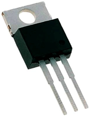
In both digital and analog circuits, mos transistors are now even more common than BJTs. The following figure shows the physical image of mos transistors.
The working principle of MOS transistor
The operation of a MOS transistor depends on the MOS capacitor, which is the semiconductor surface below the oxide layer between the source and drain electrodes. Simply apply positive or negative gate voltage separately to reverse it from p-type to n-type.
The main principle of MOSFETs is to control the voltage and current between the source and drain electrodes. Its working principle is almost like a switch, and the function of the device is based on MOS capacitors. MOS capacitors are the main part of MOS transistors.
When the drain source voltage (VDS) is connected between the drain and source, a positive voltage is applied to the drain and a negative voltage is applied to the source. Here, the PN junction of the drain is reverse biased, while the PN junction of the source is forward biased. At this stage, there will be no current flow between the drain and source electrodes.
If we apply a positive voltage (VGG) to the gate terminal, due to electrostatic attraction, a small number of charge carriers (electrons) in the P substrate will begin to accumulate at the gate contacts, forming a conductive bridge between the two n+regions.
The number of free electrons accumulated at the gate contact depends on the strength of the applied positive voltage. The higher the applied voltage, the wider the n-channel width formed by electron accumulation, which ultimately increases conductivity, and the drain current (ID) will begin to flow between the source and drain.
When no voltage is applied to the gate terminals, there will be no current flow except for a small amount of current generated by a few charge carriers. The minimum voltage at which a MOS transistor begins to conduct is called the threshold voltage.
Today's TOPCHIP Electronics class ends. If you need to learn more about MOS management, please follow our website:https://www.topchipelec.com/