Semiconductor CMOS technology has evolved over the past decade to produce high-performance systems that meet lower voltage and lower power I/O standards, especially in portable applications. Driven by low-power system design and manufacturing, many applications require a combination of I/O voltages and supply voltages. If older legacy peripherals are used in multi-voltage applications, these higher voltage devices will need to interface with the newer lower voltage application processors that are now widely available.
Nexperia's auto-sensing converters support these voltage conversion interfaces and can be used in push-pull buffered and open-drain applications.
Nexperia's voltage level translators are available in pin-compatible packages and industry-standard pin sizes with lower voltages and excellent performance. These bidirectional level translators are suitable for a variety of applications that require converting voltage signals in multiple domains and serve as an interface between different power supply and I/O voltage levels. With automatic orientation detection that eliminates the need for external orientation pins, these families are compatible with new low-voltage microprocessors.
The XS010x level converter is a switching converter that contains a single pull-up circuit that can provide better operating performance and minimal overshoot in systems with higher capacitance. This series of converters is targeted at I2C bus and other Optimized for open drain applications.
The NXB010x level translators consist of a single pull-up and pull-down circuit and are ideal as push-pull drivers for long traces, capacitive or high-impedance loads in applications using SPI, Secure Digital or UART interfaces.
Main features
1. Complete series includes 1, 2, 4, 6 and 8 channel level converters
2. Easy to use dual power conversion transceiver series
3. Bidirectional automatic detection does not require direction pins
4. Wide voltage level conversion (wide power supply voltage range)
(1)NXS
VCC(A): 1.65 V to 3.6 V and VCC(B): 2.3 V to 5.5 V
(2)NXB
VCC(A): 1.2 V to 3.6 V and VCC(B): 1.65 V to 5.5 V
5. Overvoltage tolerance input up to 5.5 V
6. Multi-pin compatible packaging options
7. The IOFF circuit provides partial power-down working mode
8. Low power consumption
9. Rated temperature range is -40 ℃ to +85 ℃ and -40 ℃ to +125 ℃
Application
1.NXS
(1)Open drain application
(2)I2C, SMBus, UART, GPIO and other telecommunications infrastructure
(3)Mobile devices and computing
(4)Car-grade version
2.NXB
(1) Application based on push-pull
(2)General portable consumer applications
(3)Bluetooth headset
(4)Mobile devices and computing
(5)Communication system
(6)Car-grade version
NXS level translators are switching converters suitable for open-drain applications. These FET-based devices use N-channel pass-gate transistors to connect two ports together (Figure 1), requiring no input signal to change direction from port A to B, or from port B to A.
The NXS converter integrates an N-channel pass FET with a 10kΩ pull-up resistor and combines it with edge rate acceleration circuitry, making it ideal for interfacing to devices or systems operating at different voltage levels while easily interfacing with open-drain drivers, compliant I2C, single wire and SD/MMC card interface application requirements.
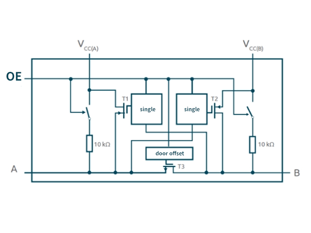
Figure 1: NXS automatic detection based on open drain
NXB level translators (Figure 2) are ideally suited as push-pull or CMOS-type drivers for driving long traces, capacitive or high-impedance loads in applications using SPI and UART interfaces.
The architecture of one I/O channel of the NXB level converter combines a weak buffer with a one-shot circuit to increase the speed of rising and falling edge transitions. For example, if the A port is connected to the system driver and driven high, the one-shot circuit triggers when it detects a rising edge and the high drive buffer drives port B high. After the single pulse is completed, the weaker 4 kΩ keeps the B port high. Driving low works the same way.
3. Output edge rate accelerator
New one-shot circuitry provides an output edge rate accelerator for the NXB/NXS family to reduce low-to-high transition times (NXS devices) or high-to-low and low-to-high conversion time (NXB devices). During the conversion process, the output one-shot circuit switches on an NMOS transistor (high to low transition) or a PMOS transistor (low to high transition). This lowers the output impedance, thereby increasing current drive capabilities and shortening output transition times. When the input transition reaches half its reference supply voltage, the one-shot circuit activates, generating a low-impedance pulse that creates a fast transient at the output.