Eliyan, a startup co-founded in 2021 by three experienced networking, connectivity, chip architecture and packaging serial entrepreneurs, recently announced details of its chiplet connectivity technology that claims to eliminate the need for advanced packaging like silicon interposers, with subsequent gains in bandwidth, power and latency for die-to-die connectivity in high-performance computing (HPC) applications.
The details were revealed as the company announced two milestones in the commercialization of its technology for multi-die chiplet integration – the successful tapeout of its technology on a TSMC 5nm process (with first silicon expected in the first quarter of 2023), and the completion of a series A $40 million funding round which includes strategic investment form Intel Capital and Micron Ventures.
The company said its design confirms Eliyan’s ability to achieve twice the bandwidth at less than half the power consumption of current interconnect methods and does so using a standard system-in-package (SIP) manufacturing and packaging process. The ability to implement chiplet-based systems in organic packages enables the creation of larger and higher performance solutions at considerably lower power and cost of materials. These factors provide major gains in sustainability.
Chiplet integration on standard substrates
As Moore’s law scaling tails off, heterogeneous chip architectures incorporating chiplets are becoming more and more common, and this then requires advanced packaging which includes EMIB (embedded multi-die interconnect bridge) and silicon interposers. Eliyan claims to have made a breakthrough with its interconnect technology that enables chiplet integration on standard substrate, using its NuLink PHY and NuGear technologies. These are said to provide a commercially viable approach to enabling high performance and cost-effectiveness in the connection of homogeneous and heterogenous architectures on a standard, organic chip substrate.

Eliyan’s chiplet connectivity technology eliminates the need for advanced packaging like silicon interposers, with subsequent gains in bandwidth, power and latency for die-to-die connectivity in high-performance computing (HPC) applications. (Image: Eliyan)
The company said these have proven to achieve similar bandwidth, power efficiency, and latency as die-to-die implementations using advanced packaging technologies, but without the other drawbacks of specialized approaches. Explaining the significance, Eliyan CEO and co-founder, Ramin Farjadrad, said, “Technology scaling using conventional system on chip (SoC) architectures is hitting the wall, requiring a new approach in how we integrate and manufacture silicon. Our extensive background in developing bleeding-edge technologies in this space led us to focus on a key challenge: interconnect improvements for system-in-package and chip-to-memory architectures as the path to deliver performance scaling. Our approach supports and is compliant with the overall industry move toward chiplet-optimized interconnect protocols, including the UCIe standard as well as high bandwidth memory (HBM) protocols.”
Eliyan co-founders from left to right: Syrus Ziai, Ramin Farjadrad, and Patrick Soheili
In an interview with Topchip electronics, Farjadrad and his co-founders Syrus Ziai and Patrick Soheili explained the importance of chiplets in HPC, and the role of chiplet-based architectures in extending beyond Moore’s Law. Utilizing the manufacturing and cost advantages of chiplets, product developers can continue to scale the performance, power efficiency and size required by high performance computing applications. Industry forecasters estimate the chiplet sector of the semiconductor market will be $50 billion, with high-bandwidth memory (HBM) applications representing an additional $8 billion market.
More efficient chiplet interconnect contributes to sustainability
The team said, “The implication of our technology is sustainability, making data centers more power efficient. By making the use of chiplets more efficient, there’s a huge implication in terms of reduction of power consumption in data centers – for example, by enabling the use of just two ASICs instead of 10 ASICs. This provides a big boost not just to performance but also sustainability. What we are doing is enabling more people to play in the chiplet game without the challenges of advanced packaging.”
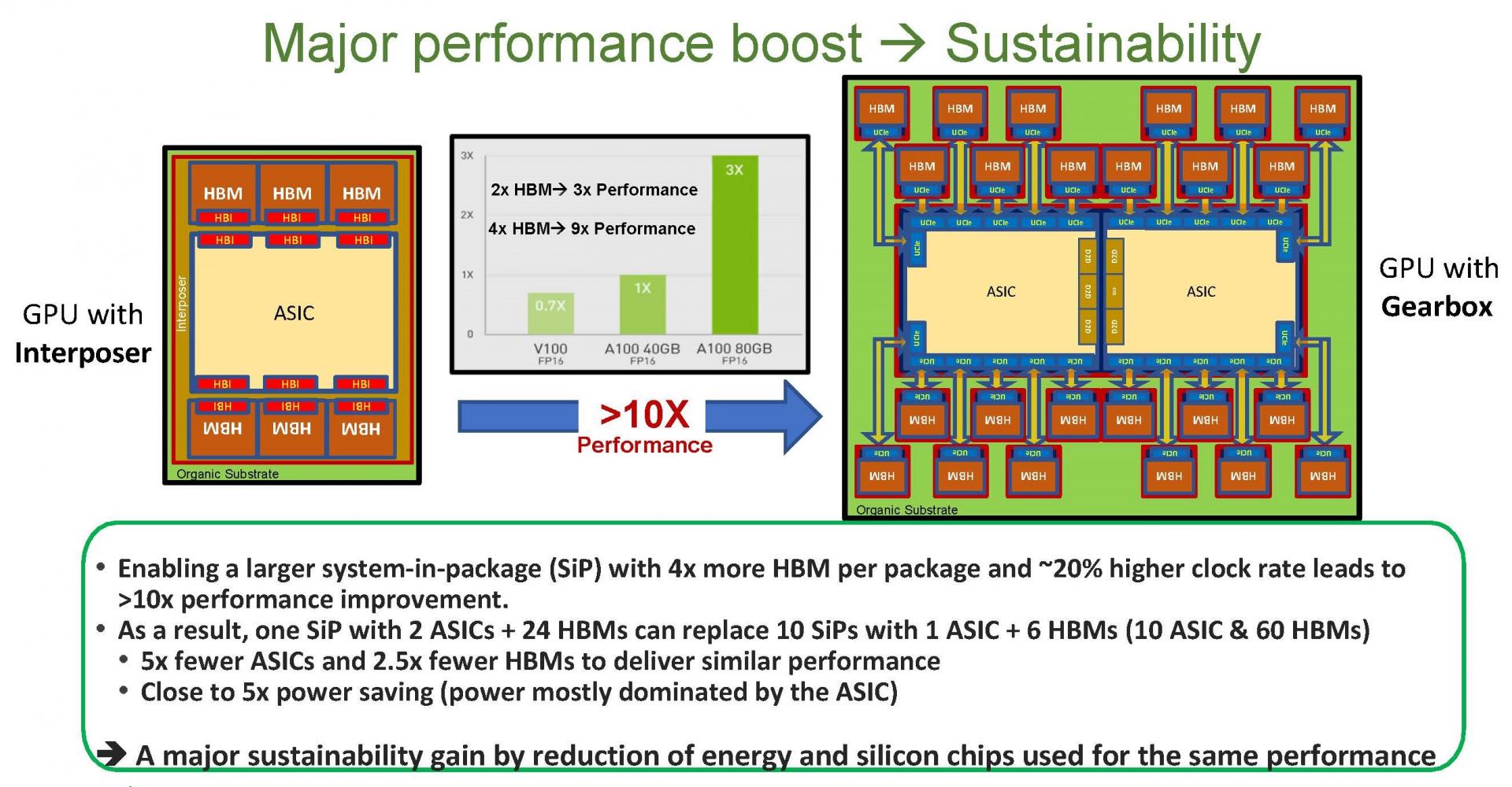
The impact of Eliyan’s D2D multi-die chiplet connectivity technology is to enable a boost in performance and efficiency, and ultimately improve sustainability. (Image: Eliyan)
Farjadrad is the inventor of the Bunch of Wires (BoW) scheme, which has been adopted by the Open Compute Project (OCP). NuLink technology is backward compatible with Universal Chiplet Interconnect Express (UCIe), a standard developed by Intel and donated to the UCIe Consortium, which includes 80+ leaders in semiconductor, packaging, foundries, cloud services and IP suppliers. Farjadrad’s experience includes pioneering work in creating connectivity technologies such as PAM4 SerDes, multi-Gbps enterprise Ethernet, and multi-Gbps automotive Ethernet that were eventually adopted as IEEE standards.
Eliyan’s BoW approach was specifically developed to address the need for highly efficient die-to-die (D2D) PHYs to connect different functions in one package. Its NuLink technology, which is a superset of BoW and UCIe, is an innovative PHY technology that uses patented implementation techniques to provide major power-performance differentiation for D2D connectivity over any packaging substrate, reducing complexity and lowering overall development time and costs. It eliminates the need for advanced packaging solutions, such as silicon interposers that limit overall system-in-package size that ultimately limits performance, results in low wafer test coverage that ultimately impacts yield, increases total cost of ownership, and extends overall manufacturing cycle time.
The company’s patented NuGear is an optimized technology for 2.5/3D implementations that enables practical mix and match of chiplets with different die-to-die interfaces in different processes (DRAM, SOI, and so on).
The technology has been under development by Farjadrad and his team since 2017. In 2018, Farjadrad proposed BoW as a superior chiplet interconnect architecture to OCP. Given the significantly improved performance and features that BoW offered over existing methods, it received strong support and later was adopted as the chiplet interconnect scheme of OCP. Farjadrad’s work not only led to the adoption of BoW at OCP, but also helped influence UCIe, which is based on the same signaling/clocking schemes and architecture basics and is widely supported in the industry.
An earlier incarnation of the NuLink technology has been mass-produced on a 14nm process, validating its commercial viability and performance advantages. The most recent version that was taped out in a TSMC 5nm process delivers a minimum of 2000Gbps/mm of edge bandwidth on a standard organic package.
Strategic investors
The $40 million series A funding round was led by Tracker Capital with additional investment from Celesta Capital and strategic investors including Intel Capital and Micron Ventures. As part of the investment from Tracker Capital, made in February 2022, Dr. Shaygan Kheradpir of Cerberus, former group CIO and a founding member of the executive leadership committee at Verizon, is joining the board of directors of Eliyan.
Kheradpir commented,“Traditional methods of integrating multi-chip architectures impose challenges that result in high costs, low yield, manufacturing complexity, and size limitations. Eliyan has drawn upon its years of experience to develop a practical scheme that is also backward compatible with existing standards to chiplet interconnect and is optimized for delivering the necessary high bandwidth, low latency, and low power capabilities. We are confident its NuLink technology holds the key to a broader proliferation of chiplets in key market sectors such as hyperscalers, AI processor development, high-performance memory, and advanced graphics chips.”