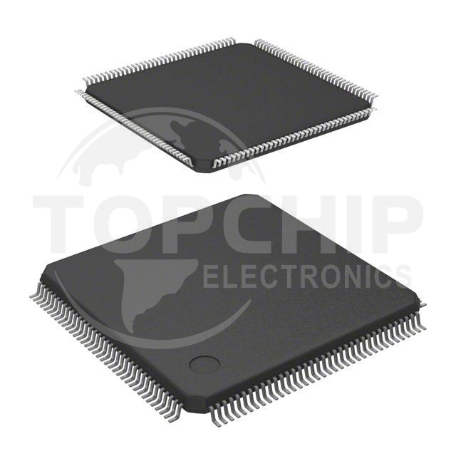
STM32F407ZET6 is a high-performance 32-bit microcontroller (MCU) launched by STMicroelectronics. Its rich peripheral resources and flexibility make it an ideal choice for embedded systems. However, to realize the full potential of the STM32F407ZET6, a well-designed peripheral circuit is crucial. STMicroelectronics agents will introduce key aspects of STM32F407ZET6 peripheral circuit design.

1. Clock circuit design
The clock system of STM32F407ZET6 is the basis for the normal operation of the entire chip. In the peripheral circuit design, it is necessary to ensure that a suitable clock source is provided for STM32F407ZET6. Usually, you can choose to use an external crystal oscillator or use an internal clock source to configure it appropriately according to the needs of the specific application. The design of the clock circuit should ensure the stability and accuracy of the clock to ensure the normal operation of the MCU.
2. Power circuit design
A carefully designed power circuit is crucial to the stable operation of STM32F407ZET6. Use appropriate voltage regulators and capacitors to ensure that the chip supply voltage is within the specified range and prevent power supply noise and fluctuations from affecting chip performance. In addition, for low-power applications, the power management module can be reasonably configured to reduce power consumption.
3. Reset circuit design
The reset circuit is a critical part of ensuring proper system operation at startup. Provide appropriate reset circuits for STM32F407ZET6, including reset buttons, power-on reset circuits, etc., to ensure that the system can reliably start from the reset state.
4. Peripheral connection
Peripheral circuit design should take into account the rich peripheral resources of STM32F407ZET6, including GPIO, UART, SPI, I2C, etc. Designers need to properly configure the pins of these peripherals and ensure level matching between the peripherals and STM32F407ZET6 through level converters and other methods.
5. Debugging and programming interface
In the peripheral circuit, debugging and programming interfaces need to be set aside to facilitate connection during development and debugging. Usually JTAG or SWD interfaces are used for debugging and programming, and designers should ensure the reliability and convenience of these interfaces.
6. External memory interface
If the application requires a large amount of storage space, the peripheral circuit design needs to consider connecting external memory, such as NAND Flash, SD card, etc. Provide appropriate circuits and interfaces for these external memories to ensure that STM32F407ZET6 can communicate with them stably.
7. Analog circuit design
STM32F407ZET6 has built-in analog modules, including analog input, analog output and analog-to-digital converters (ADC and DAC). In peripheral circuit design, these analog circuits need to be properly designed and connected to meet the analog signal processing needs of specific applications.
8. Layout and hierarchy of peripheral circuits
Board layout is critical to system performance and stability. Properly layout the circuit to avoid interference between digital and analog signals, and adopt appropriate hierarchical design to ensure that power supplies, clocks, signal lines, etc. are arranged in an orderly and clear manner, which will help improve system performance and anti-interference capabilities.
STM32F407ZET6 is a powerful MCU, and the design of its peripheral circuits directly affects the performance and stability of the system. Carefully designed clocks, power supplies, resets, peripheral connections, debug interfaces, external memory interfaces, analog circuits, and circuit board layout ensure that the STM32F407ZET6 performs well in a variety of applications. Designers should carefully weigh the specific application requirements and hardware characteristics when designing peripheral circuits to achieve optimal performance and stability.
If you need data manuals, sample testing, procurement, BOM ordering, etc., please contact us via the following email address:

